

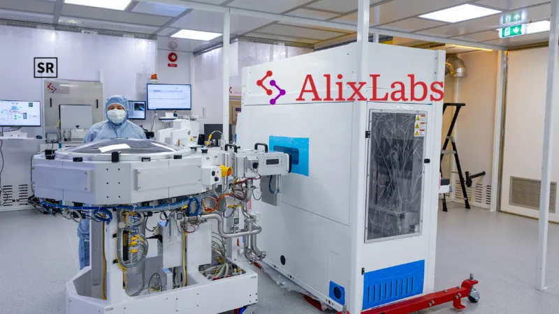
AlixLabs, a semiconductor manufacturing solutions company based in Lund, Sweden, has raised €14.1 million in Series A funding.
SUMMARY
- AlixLabs, a semiconductor manufacturing solutions company based in Lund, Sweden, has raised €14.1 million in Series A funding.
 Follow us
 Follow us
The Series A round was led by Navigare Ventures, Industrifonden, and FORWARD.one, with additional participation from Sweden’s STOAF and Global Brain.
AlixLabs plans to use the funding to accelerate the development and scaling of its proprietary Atomic Layer Etching Pitch Splitting (APS) technology.
Read Also - Model ML Raises €65 M Its AI Beats McKinsey And Bain Benchmarks With Under-3-minute Output Checks
RECOMMENDED FOR YOU
[Funding alert] Rotterdam-based SolarDuck Secures €15 Million in Funding
Oliver Bennett
Dec 21, 2023

Ralio Raises €2.1M Pre-Seed Funding To Build AI Payment Platform In London
Oliver Bennett
Apr 14, 2026
Led by CEO Jonas Sundqvist, AlixLabs is a deep-tech company spun out of Lund University, developing atomic layer etching (ALE) technology known as ALE Pitch Splitting (APS).
The company claims its APS method enables more cost-effective, sustainable, and efficient semiconductor fabrication by splitting nanostructures in a single process step.
APS beta testing with customers is scheduled to begin in 2026, with early manufacturing implementation targeted for 2027.
“This Series A enables us to transform our APS™ innovation from customer validation to industrial adoption,” said Jonas Sundqvist CEO of AlixLabs. “We’re now entering an exciting phase where our focus turns toward beta testing with leading customers – a critical step on the path to full-scale manufacturing by 2027. Our technology has the potential to dramatically lower both energy use and costs per wafer, helping to make advanced semiconductor production more accessible.”
About AlixLabs
AlixLabs is a Swedish semiconductor supplier offering equipment and processes for manufacturing nanostructures smaller than 20 nanometers. Using APS™, the company enables energy-efficient fabrication of structures beyond the resolution limits of optical and electron beam lithography.
Recommended Stories for You

Oliver Bennett May 19, 2026

Kailee Rainse Aug 20, 2025
Oliver Bennett Jul 29, 2026
Oliver Bennett Sep 24, 2024
Kailee Rainse Mar 6, 2026
Oliver Bennett Nov 21, 2023
Trending Stories
Acurast Raises $11M to Redefine Computing With A Smartphone-Driven Network
ZettaScale funding news – ZettaScale Launches a Funding Round to Accelerate Growth in Disruptive Connectivity Solutions

[Funding alert] German Deep Tech Startup Orbem has Raises €30M in its Series A Round Funding
Phyron funding news- Stockholm-based Phyron Secures €10Million in Series B Round Funding

Lytra Closes Pre-Seed Round To Expand AI Manufacturing Solution

Oh funding news – UK-based Oh Secures $4.5 Million in Seed Funding

[Funding alert] Custom Products Platform Bizay Secures € 18 Million in Series C2 Round Funding
iPronics funding news – Valencia-based Deeptech startup iPronics Secures €20Million in Series A Round Funding